PES met up with Frederick Bamberg, Product Manager at 3D-Micromac AG in Chemnitz, Germany, to discover the advances in laser machines and processes in relation to the PV industry. Efficiency and cost savings are being achieved through listening to the customer, R&D and expertise.
PES: Welcome back to PES Solar/PV magazine. For the benefit of our new readers would you like to begin by explaining a little about the importance of the solar industry to 3D-Micromac?
Frederick Bamberg: The PV industry is one of our key markets and accounts for approximately 30% of our business. Within in few years 3D-Micromac succeeded in establishing itself amongst the Top 3 manufacturers of laser equipment in the solar industry.
We offer different machine concepts for the various fields of the PV industry. For example, our customers in the c-Si/wafer based segment prefer our microCELL OTF and microCELL TLS platforms for PERC-LCO, innovative cell cutting as well as doping. Those in the TFPV segment prefer the microSTRUCT LS for thin films on glass panels as well as the microFLEX family for thin films on flexible substrates.
Apart from these established mass production tools, we also offer fully flexible platforms to R&D centres in the sector. Currently we are also working on an elaborate, fully customised tool, for a special PV pilot line. The customer benefits from this broad variety of expertise and process know how.
PES: We would like to know what makes your laser equipment stand out from the competition?
FB: Our philosophy is completely different from our competitors. We grant the customer a much wider flexibility; our platforms match precisely the specific needs.
Also they are far from being just a rebuild or simplified version of existing tool concepts, as is often the case.
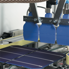
When designing the microCELL concept we looked at the disadvantages of current systems on the market and gathered feedback from production engineers and operators about their most important but, to date, unmet expectations. So with this tool concept, the customer benefits from a basically contact less wafer transportation, as well as processing in continuous motion. The benefits are obvious: scratches and micro cracks are avoided while the throughput is boosted by ~20%.

