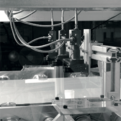
Optical integrated metrology systems enable rapid and non-destructive process and quality control during the production of thin film photovoltaic (PV) devices. Given today’s price pressure, and the increasing complexity of the device architecture and process sequences, such methods become mandatory for economic thin film PV device manufacturing. Both technological and financial aspects have to be considered when selecting the most appropriate system for a production line, to ensure that the product quality benefits the most from it.
In recent years, record efficiencies of thin film PV devices have increased rapidly1 and record efficiencies for CIGS, CdTe, and perovskite devices approached or even surpassed those of multi-crystalline silicon. In the case of silicon/perovskite tandem devices, even the best monocrystalline silicon monojunction devices have been outperformed. Currently, no end of this trend is visible. Rather more, these developments have resparked commercialization.
The last years have seen several major investments in thin film PV in CIGS, CdTe and perovskites and several CdTe and CIGS manufacturers are currently rolling out their technologies approaching or surpassing the GW level. As price pressure remains tremendous especially in thin film PV, these new fabs must be designed for maximum cost efficiency. A fully automated quality control system ensuring that the consumed materials result in the maximum number of modules at maximum product quality becomes mandatory.
Today, thin film PV processes become more complex in order to drive device efficiency towards its physical maximum. An increasing number of layers in the device stacks and additional pre- and post-deposition treatments are added and intentional material gradients are introduced. Additionally, the windows for all parameters such as temperature, purity, evaporation rate etc. become tighter.
1 https://www.nrel.gov/pv/cell-efficiency.html


