Dutch specialist PV equipment manufacturer Levitech has developed a system that allowed mono-crystalline wafers to break the 20% efficiency barrier, resulting in considerable cost-of-ownership savings for high-volume solar cell manufacturers. Now they are able to demonstrate that this technology can extend to multi-crystalline wafers, taking them through the 19.5% barrier.
Over the last several years, various types of Atomic Layer Deposition (ALD) films have been successfully introduced into high-volume manufacturing in a number of industries. More recently, a specific type of ALD film, Al2O3, has demonstrated great ability as a surface passivation layer for solar cells.
Thin (less than 10 nanometres) Al2O3 films are able to passivate p-type surfaces very effectively, as intrinsic negative charges in the dielectric film repel charge carriers, while the hydrogen present in the ALD films passivates dangling bonds at the Si/SiO2/Al2O3 interface. The combination of both effects results in an increase in cell efficiency of 0.5-1% point to more than 20% (absolute) in mono-crystalline wafers.
Following extensive testing, Al2O3 films are now being implemented in high-volume PV manufacturing, the only type of ALD film being introduced into the solar cells manufacturing industry at this time. This is due not only to its excellent surface passivation capabilities, but also to the fact that it is probably the only ALD film that can be deposited at a cost considered acceptable to the PV industry.
“Over the past year, the solar industry has embraced Atomic Layer Deposition as a mass production solution for maximising solar cell efficiencies,” Levitech CEO Jaap Beijersbergen said. “Aluminium oxide (Al2O3) film provides excellent cell passivation and increased cell efficiencies, especially when deposited in uniform, pinhole-free and dense layers. This is a particular feature of the ALD technique and in the Levitrack these qualities are combined with an efficient and effective platform for mass production.” This is confirmed by the recently announced tool orders.
The benefits of spatial ALD
The method by which the ALD film is deposited on the wafers plays a significant role in the technology’s cost effectiveness. In temporal or conventional ALD, the substrate is kept at a fixed position, while the pre-cursor and inert gas supplies are pulsed in time. In that way, the substrate is exposed to a specific sequence of precursor exposures (precursor 1, inert gas, precursor 2, inert gas, etc.).
In spatial ALD, the roles of time and place are inverted. Precursors flow continuously, but are injected at spatially different positions (typically at 1 atm pressure). The substrate is then exposed to the same sequence of precursors by moving it through space from one precursor injection area to the next.
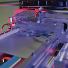
This technique is applied in Levitech’s Levitrack system. Here, wafers are loaded onto a track which has TMA and H2O injection zones spatially separated by zones of inert gas (N2) (called an ALD cell). When the gas flow is above a well-defined level, the wafers will float, kept in position by strong forces from above and below. Lastly, the reactor is installed at a slight angle, which allows the floating wafers to move down along the track through gravity.
The system is designed such that, as the wafers pass through ALD cells that each add a thin layer of Al2O3, the different precursors do not mix. Therefore, independent of the presence of wafers, deposition only takes place on objects that pass the subsequent precursor zones. As there is no belt carrying the wafers, no deposition takes place on wafer carriers.
At a growth rate at 200 degrees Celsius of 0.12 nm per cycle, one nm of Al2O3 is deposited on each metre of ‘active’ length. The wafers travel with a typical velocity of 0.2 m per second. When wafers are injected with a pitch of 25 cm, the throughput is 3,000 wafers per hour.
In addition to a high throughput, this approach has several other advantages: as the process takes place under atmospheric pressure, no pumps or valves are required. The volume of the reactor in which the substrates are exposed to the precursors is very small, which increases the TMA efficiency significantly. Further, no moving parts are present in the deposition section of the track. Together, this results in an excellent reliability and cost-of-ownership.
Process improvements for PERC
The new process by which PERC (passivated emitter and rear cell) mono-crystalline cells are coated with Al2O3 back-side surface passivation films has further benefits. PERC cells are prepared by: texturising both the front and back sides of the wafers; dopant diffusion; adding SiNx Anti-Reflective coating on the front side; and the Al2O3 passivation and SiNx capping layers on the back side.
Then the Al2O3/SiNx stack is removed locally with a fast-pulsed laser, after which Al metallisation paste is screen-printed and fired. The Al paste penetrates the laser-ablated holes in the dielectric stack and reacts with the Si substrate to form the local Al- BSF contact (Back-Surface Field).
Formerly, the back side needed to be polished before adding the Al2O3/SiNx stack, but now the step coverage and the surface-passivation capabilities of the ALD Al2O3 film are so good that the back-side polishing step can be omitted. This omission results in a considerable cost saving and is currently being looked at seriously in the industry.
The optimisation of the different process steps for PERC cells has resulted an efficiency of 20.2% on average for industrial mono-crystalline Si wafers.
Expanding to multi-crystalline wafers
For multi-crystalline wafer production, cost-of-ownership is of even greater importance, given the fact that it is a lower cost product. Currently, the efficiency average for the state-of-the-art, full-Al BSF multi-crystalline cells is 18.5%.
This barrier has been broken, however, thanks to experimentation with the Levitrack system. The system’s cost-of-ownership benefits had garnered such interest from high-volume manufactures that one of Levitech’s customers, which already had a system in place for mono-crystalline wafer production, started experimenting with PERC process flow for multi-crystalline wafers.
Simply putting PERC through the mono-crystalline process flow resulted in efficiencies in the 19% range, already above previous highest level. By further optimising the process and process sequences for multi-crystalline wafers, they were able to achieve 19.5%. They also calculated that as the Levitrack’s cost-of-ownership is so low and the increase in efficiency was so great, they would be able to increase their gross margin on sales up to a factor of 2.
“We’re very excited by these results,” says Beijersbergen. “Also because they come out of our partnership with a customer. These are the kinds of results that enable growth, for us, for our customers and for the industry. It shows that PERC with ALD is definitely the frontrunner in solar cell solutions.”