Balancing cell- and cost-efficiency InnoLas Systems laser PERC solution offers up to 3,600 wafers per hour throughput See InnoLas Systems at SNEC PV Power Expo, Shanghai, Booth E3 398
One of the most effective ways to reduce the cost of solar power is increasing cell efficiency. It lowers the cost per watt of solar panels and also reduces installation costs, because fewer solar panels are needed to achieve a given output.
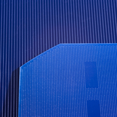
At the current state of development, PERC (Passivated Emitter and Rear Contact) is the only cell power increasing technology that meets the balance between manufacturing cost and efficiency, while providing an acceptable payback time of investment. With the highly integrated ILS TT, InnoLas Systems offers cell manufacturers a mature machine platform, perfectly suited to upgrading existing production lines. It offers the necessary laser processes to increase efficiency and also to lower overall operating costs. The InnoLas solution consists of the ILS TT basis platform and a matched InnoLas Systems handling unit. What sets the ILS TT apart from other systems on the market is the very high throughput of up to 3,600 wafers per hour. (The actual throughput in an installation depends on the design of the opening for the rear passivation layer) Different laser sources are available for the ILS TT to optimize the system for individual process requirements. InnoLas Systems offers a fully equipped application lab, skilled experts and more than 20 years of experience in laser technology to help customers find the best laser solution for a given process. In the case of PERC technology, the laser source is chosen according to the design for the opening of the rear passivation layer. The most common design is a “line pattern” where 30-50µm wide grooves form the contact area and BSF (Back Surface Field). A “dot pattern” geometry utilizes a grid of circular openings with >80µm diameter. The contact formation is more challenging, but it allows for optimization of series resistance and short circuit current. Richard Grundmüller, CEO InnoLas: “Our ILS TT solution is unique in that it offers a throughput of up to 3,600 wafers per hour for both, line pattern and dot pattern PERC. Until today, we have installed systems for a production capacity of +1.5 GW/year. This proofs that our concept is production-ready and does offer clear advantages to our customers. More than 75 ILS TT systems are currently used in large and small facilities all across the world. In addition to PERC technology InnoLas Systems also installed production machines for laser selective emitter technology, laser edge isolation, MWT drilling and pad isolation, laser fired contacts, and IBC cell processing. We have the know-how and experience to combine different laser processes into a complete concept that can push efficiencies over 20%.”
About InnoLas Systems GmbH InnoLas Systems GmbH produces laser systems for micro material processing, particularly in the photovoltaic industry, for semiconductors, electronics and precision engineering. InnoLas Systems designs and manufactures machinery solutions as stand-alone systems or for inline integration, perfectly adapted to industrial production conditions. Worldwide service and support ensures smooth setup and reliable operation. InnoLas Systems utilizes innovations in laser technology to produce highly-efficient and reliable processing systems.
Reader inquiries: InnoLas Systems GmbH Robert-Stirling-Ring 2 82152 Krailling Germany Tel: +49 89 899 4828-0 Email: info@innolas-systems.com

