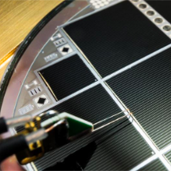
FREIBURG, Germany and ST. FLORIAN, Austria, November 9, 2016–Researchers at the Fraunhofer Institute for Solar Energy Systems ISE together with the Austrian company EV Group (EVG) have successfully manufactured a silicon-based multi-junction solar cell with two contacts and an efficiency exceeding the theoretical limit of silicon solar cells. For this achievement, the researchers used a “direct wafer bonding” process to transfer a few micrometers of III-V semiconductor material to silicon, a well-known process in the microelectronics industry. After plasma activation, the subcell surfaces are bonded together in vacuum by applying pressure. The atoms on the surface of the III-V subcell form bonds with the silicon atoms, creating a monolithic device. The efficiency achieved by the researchers presents a first-time result for this type of fully integrated silicon-based multi-junction solar cell. The complexity of its inner structure is not evident from its outer appearance: the cell has a simple front and rear contact just as a conventional silicon solar cell and therefore can be integrated into photovoltaic modules in the same manner.
“We are working on methods to surpass the theoretical limits of silicon solar cells,” says Dr. Frank Dimroth, department head at Fraunhofer ISE. “It is our long-standing experience with silicon and III-V technologies that has enabled us to reach this milestone today.” A conversion efficiency of 30.2 percent for the III-V / Si multi-junction solar cell of 4 cm² was measured at Fraunhofer ISE’s calibration laboratory. In comparison, the highest efficiency measured to date for a pure silicon solar cell is 26.3 percent, and the theoretical efficiency limit is 29.4 percent.
The III-V / Si multi-junction solar cell consists of a sequence of subcells stacked on top of each other. So-called “tunnel diodes” internally connect the three subcells made of gallium-indium-phosphide (GaInP), gallium-arsenide (GaAs) and silicon (Si), which span the absorption range of the sun’s spectrum. The GaInP top cell absorbs radiation between 300 and 670 nm. The middle GaAs subcell absorbs radiation between 500 and 890 nm and the bottom Si subcell between 650 and 1180 nm, respectively. The III-V layers are first epitaxially deposited on a GaAs substrate and then bonded to a silicon solar cell structure. Subsequently the GaAs substrate is removed, and a front and rear contact as well as an antireflection coating are applied. “Key to the success was to find a manufacturing process for silicon solar cells that produces a smooth and highly doped surface which is suitable for wafer bonding as well as accounts for the different needs of silicon and the applied III-V semiconductors,” explains Dr. Jan Benick, team leader at Fraunhofer ISE. “In developing the process, we relied on our decades of research experience in the development of highest efficiency silicon solar cells.” Institute Director Prof. Eicke Weber expresses his delight: “I am pleased that Fraunhofer ISE has so convincingly succeeded in breaking through the glass ceiling of 30 percent efficiency with its fully integrated silicon-based solar cell with two contacts. With this achievement, we have opened the door for further efficiency improvements for cells based on the long-proven silicon material.”
“The III-V / Si multi-junction solar cell is an impressive demonstration of the possibilities of our ComBond® cluster for resistance-free bonding of different semiconductors without the use of adhesives,” says Markus Wimplinger, Corporate Technology Development and IP Director at EV Group. “Since 2012, we have been working closely with Fraunhofer ISE on this development and today are proud of our team’s excellent achievements.” The direct wafer-bonding process is already used in the microelectronics industry to manufacture computer chips.
On the way to the industrial manufacturing of III-V / Si multi-junction solar cells, the costs of the III-V epitaxy and the connecting technology with silicon must be reduced. There are still great challenges to overcome in this area, which the Fraunhofer ISE researchers intend to solve through future investigations. Fraunhofer ISE’s new Center for High Efficiency Solar Cells, presently being constructed in Freiburg, will provide them with the perfect setting for developing next-generation III-V and silicon solar cell technologies. The ultimate objective is to make high efficiency solar PV modules with efficiencies of over 30 percent possible in the future.
Project Sponsorship
The young researcher Dr. Romain Cariou carried out research on this project at Fraunhofer ISE with the support of a Marie Curie Postdoctoral Fellowship. Funding was provided by the EU project HISTORIC. The work at EVG was supported by the Austrian Ministry for Technology.
Text of the PR and photos can be downloaded from www.ise.fraunhofer.de
About Fraunhofer ISE
With a staff of 1100, the Fraunhofer Institute for Solar Energy Systems ISE, based in Freiburg, is the largest solar energy research institute in Europe. Fraunhofer ISE is committed to promoting energy supply systems which are sustainable, economic, safe and socially just. It creates the technological foundations for supplying energy efficiently and on an environmentally sound basis in industrialized, threshold and developing countries. To this end, the institute develops materials, components, systems and processes within a total of five different business areas. Fraunhofer ISE also has numerous accredited test facilities and other service facilities. The institute is a member of the Fraunhofer-Gesellschaft, the largest organization for applied research in Europe. For more information, visit www.ise.fraunhofer.de.
About EV Group (EVG)
EV Group (EVG) is a leading supplier of equipment and process solutions for the manufacture of semiconductors, microelectromechanical systems (MEMS), compound semiconductors, power devices and nanotechnology devices. Key products include wafer bonding, thin-wafer processing, lithography/nanoimprint lithography (NIL) and metrology equipment, as well as photoresist coaters, cleaners and inspection systems. Founded in 1980, EV Group services and supports an elaborate network of global customers and partners all over the world. More information about EVG is available at www.EVGroup.com.

