The German family-owned company VON ARDENNE develops and manufactures advanced vacuum coating equipment for the photovoltaic and solar thermal industry, the architectural glass coating market, and the web coating market. We take a closer look at the company, which is constantly identifying and analysing market trends throughout these industries in order to strengthen and broaden its technology portfolio.
Today, VON ARDENNE’s key technologies are magnetron sputtering and electron beam evaporation and it holds more than 600 patents worldwide. However, the company was founded in 1991 as a spin-off of the former Manfred von Ardenne Research Institute in Dresden, Germany. A consequence of this was that the expertise in plasma and electron beam technologies that had been acquired over decades could be used and developed further.
The company owes its name to Manfred von Ardenne, a highly gifted, visionary and tenacious scientist and inventor born in 1907. His contribution to inventions such as the radio receiver, the television, and the scanning electron microscope is extraordinary. He held approximately 600 patents in radio and television technology, electron microscopy, nuclear plasma, and medical technologies and was the author of countless books and publications – all done without holding a degree or even a high school diploma. It was thanks to his farsightedness and hard work that he progressed from school dropout to famous scientist.
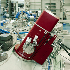
Today, VON ARDENNE offers high precision vacuum coating equipment such as the PIA|nova coating platform. It is an industry-proven solution for applying thin metal and transparent oxide (TCO) layers on thin-film and wafer based solar cells. The main applications are functional layers for:
Copper indium and gallium (CIGS) thin-film cells
i) back contacts based on molybdenum including different barrier layers
ii) precursor based on copper,
indium and gallium for all technologies using a sequential precursor and selenisation process
iii) front contacts based on intrinsic zinc oxide and aluminum doped zinc oxide
Cadmium telluride and silicon based thin film cells
i) back contacts based on different metals
Crystalline solar cells using hetero junction with intrinsic thin layer (HIT) technology
i) transparent conductive oxides
ii) metal contact layers

